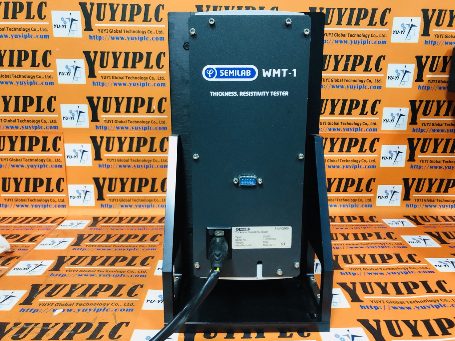
SEMILAB WMT-1 SILICON PV WAFERS THICKNESS AND RESISTIVITY MEASUREMENT
Thickness is a primary control parameter of silicon PV wafers. By filtering out wafers with non-standard thickness and shape, waste from wafer/cell breaking can be reduced.
Thickness of PV wafers is measured for two reasons:
1.To insure specification. From the thickness measured in different points of the wafer, the following parameters can be calculated:
- Average thickness
- Total Thickness variation (TTV)
- Thickness Deviation
2.To obtain resistivity value by using the Eddy current technique based on thickness information to report the bulk resistivity of the sample.
DATA:SEMILAB |