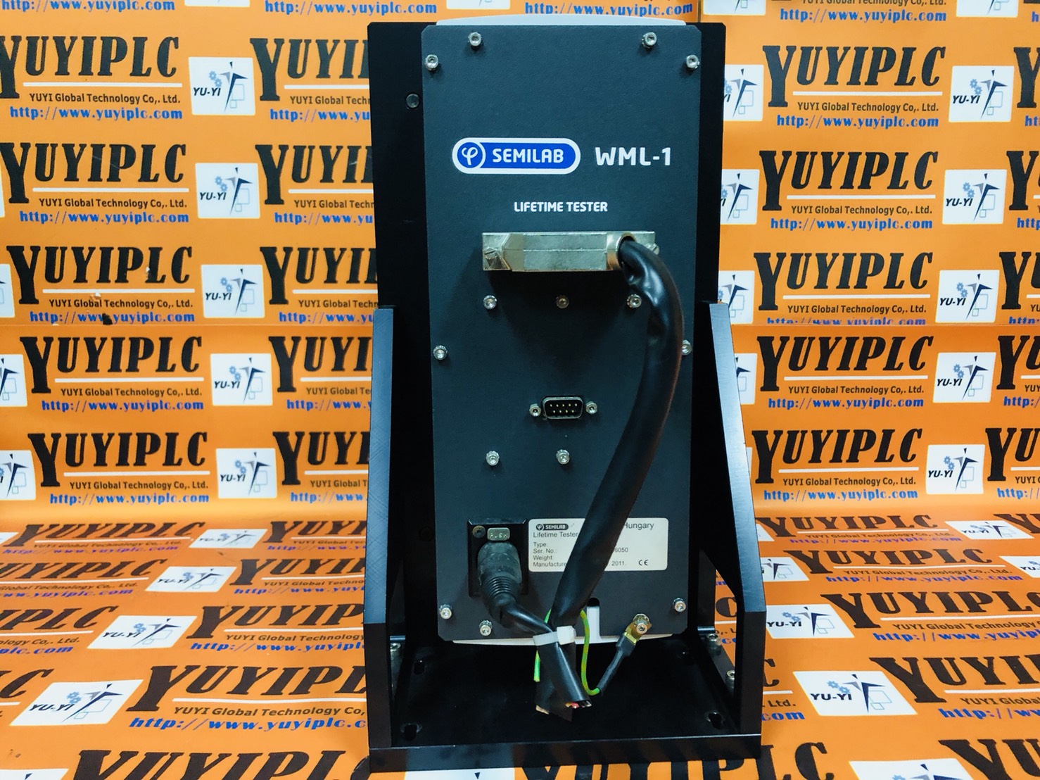
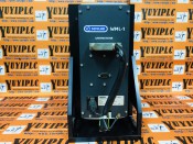
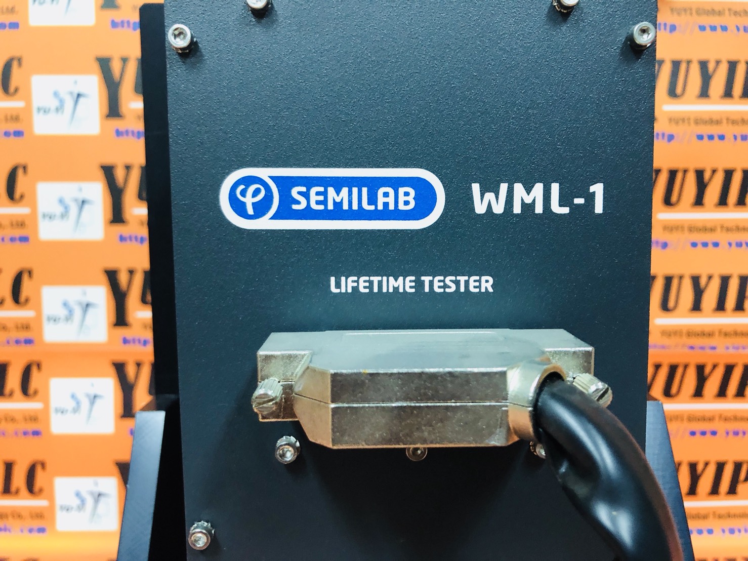
SEMILAB WML-1 SILICON PV WAFERS THICKNESS AND RESISTIVITY MEASUREMENT
Thickness is a primary control parameter of silicon PV wafers. By filtering out wafers with non-standard thickness and shape, waste from wafer/cell breaking can be reduced.
Thickness of PV wafers is measured for two reasons:
1.To insure specification. From the thickness measured in different points of the wafer, the following parameters can be calculated:
- Average thickness
- Total Thickness variation (TTV)
- Thickness Deviation
2.To obtain resistivity value by using the Eddy current technique based on thickness information to report the bulk resistivity of the sample.
for silicon wafers in PV applications. The WML models, WML-1 & WML-3, Lifetime Testers allow measurement of wafers “on the fly,"
DATA:SEMILAB |